The Michael J. Drake
Electron Microprobe Laboratory
University of Arizona
Electron Microprobe Capabilities
Quantitative
Analysis
Qualitative Analysis-
(WDS Scanning)
(EDS)
X-ray Mapping
Backscattered
Electron Imaging
Secondary Electron
Imaging
Absorbed Current
Imaging
Quantitative Analysis
The main function of an electron microprobe is to perform quantitative analysis using wavelength dispersive spectrometry (WDS). This technique provides accurate, non-destructive, quantitative chemical analyses of areas a few microns in size in solid materials. Most solid materials can be analyzed if properly prepared. Samples ranging in width from a few 100s of microns to up to ~ 50 mm (2.5") can be accommodated in our microprobe.
High-quality WDS analysis requires a stable well maintained instrument as well as a suite of reliable, well characterized standards. The CAMECA SX100 in our lab has been maintained under a full service contract with the manufacturer throughout its lifetime and has proven to be exceptionally stable over that time. The CAMECA SX50 also still provides reliable analyses. The lab maintains a diverse and ever growing collection of almost 300 natural and synthetic standards to provide for the analysis of a wide range of different materials.
The minimum detection limits (MDL) and analytical accuracy of a WDS analysis depends in large part on the electron beam conditions and counting times chosen for the analysis (although other factors can also be significant in certain situations). A typical geochemical analysis on our instrument for 11 elements under conditions of 15 keV accelerating voltage, 20 nA beam current, 2 μm beam size, and 30 second peak count time would require ~4 min per analysis and would yield MDLs of ~100 - 300 ppm (3σ) for all elements and a 1σ accuracy of 0.5 - 1.5% relative for major elements (those present at concentrations > 1 wt%). MDLs and 1σ errors could both be improved (if desired) by increasing counting times, beam current, or both. Light elements (Z < 9) are more difficult to analyze on the electron microprobe and analyses for these elements have larger MDLs and 1σ errors than do analyses for heavier elements made under the same conditions.
Our microprobe is often used for trace element analysis (elements present at concentrations < 0.1 wt%) using higher accelerating voltages, beam currents, and counting times. Accelerating voltages of up 25 keV and regulated beam currents up to 300 nA can be employed on suitable samples (unregulated beam currents of 300 - 800 nA are also possible) and can produce MDLs as low as 5 ppm in favorable cases.
Computer automated analysis allows users to set up points, lines, or a combination of both to be analyzed unattended at a later time (usually overnight). Results are given in one or more custom, tab-delimited reports which are compatible with any spreadsheet program.
Our CAMECA SX50 is equipped with four WDS spectrometers containing 12 diffracting crystals which allow analysis of all elements with Z ≥ 4 (beryllium). The spectrometer configuration of our SX50 is shown below.
| Crystal | 2d (Ĺ) | Formula | Verify | K-Shell Range | L-Shell Range | M-Shell Range | |||||||||||||||||||||||||||||
| Spectro
1 1 Atm P10 polypropylene window |
|
||||||||||||||||||||||||||||||||||
| Spectro
2 1 Atm P10 polypropylene window |
|
||||||||||||||||||||||||||||||||||
| Spectro
3 3 Atm P10 mylar window |
|
||||||||||||||||||||||||||||||||||
| Spectro
4 3 Atm P10 mylar window |
|
||||||||||||||||||||||||||||||||||
Our CAMECA SX100 is equipped with five WDS spectrometers containing 14 diffracting crystals which allow analysis of all elements with Z ≥ 5 (boron). Three of the spectrometers are equiped with large LPET and LLIF crystals which provide more counts and better peak-background ratios than do normal sized crystals of the same type. The spectrometer configuration of our SX100 is as follows.
| Crystal | 2d (Ĺ) | Formula | Verify | K-Shell Range | L-Shell Range | M-Shell Range | |||||||||||||||||||||||||||||
| Spectro
1 1 Atm P10 polypropylene window |
|
||||||||||||||||||||||||||||||||||
| Spectro
2 3 Atm P10 mylar window |
|
||||||||||||||||||||||||||||||||||
| Spectro
3 3 Atm P10 mylar window |
|
||||||||||||||||||||||||||||||||||
| Spectro
4 1 Atm P10 polypropylene window |
|
||||||||||||||||||||||||||||||||||
| Spectro
5 3 Atm P10 mylar window |
|
||||||||||||||||||||||||||||||||||
Qualitative Analysis
Two methods are available for rapid qualitative determination of the elements present and estimation of their relative abundances in an unknown sample, WDS scanning and energy dispersive spectrometry (EDS). Both methods are based on analyzing the spectra of characteristic x-rays emitted by the specimen. Applications where these techniques are useful include rapid phase identification, qualitative determination of the presence or absence of major or trace elements, and the determination of interferences and background positions needed for subsequent quantitative analysis by WDS analysis.

WDS Scanning
In this method the crystals in the WDS spectrometers are scanned over a predetermined wavelength range and the intensity of the x-rays detected plotted vs. wavelength (or energy). The elements present are identified by peak matching. WDS analysis is particularly useful for determining the presence of trace elements (< 0.1 wt%) in an unknown sample and also for identifying suitable background positions and potential interferences for WDS analysis. A reasonable full scan for all elements from B to U can be obtained in approximately 10 minutes. Longer dwell times, repeat scanning, and smaller wavelength ranges can be used for better resolution or for elements present in very low concentrations.
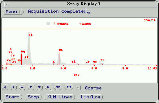
EDS (Energy Dispersive Spectrometry)
Our microprobe is equipped with a venerable PGT-5000 EDS detector. The detector simultaneously collects all x-ray wavelengths emitted from the sample and displays an intensity vs. energy (or wavelength) spectra in a matter of a few seconds. The elements present are identified by peak matching. This method is very useful for quickly identifying phases and minerals by pattern matching, rapid determination of the presence or absence of an element, and qualitative analysis of non-flat samples. However, x-ray resolution and peak-background ratios are significantly lower than can be obtained by WDS scanning, and on our system, detection is limited to elements with Z > 9 and present in concentrations >1 wt%.
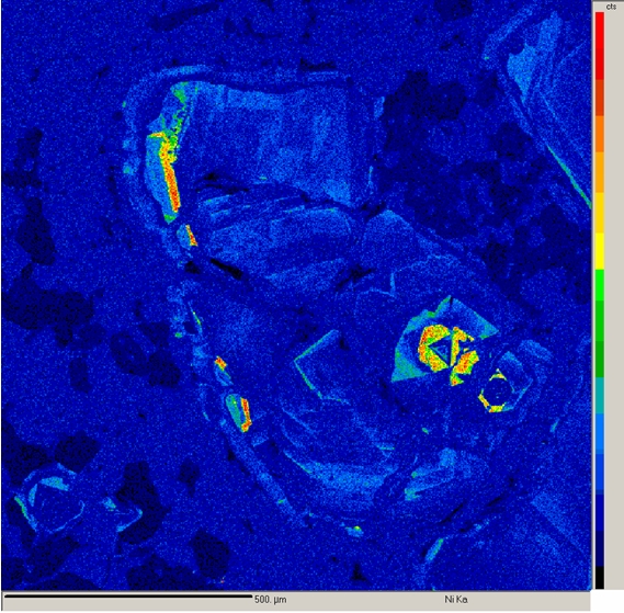
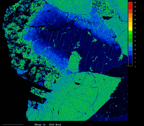
X-ray Mapping
X-ray mapping is a powerful technique that allows imaging the spatial distribution of chemical elements within a sample. It is extremely useful for revealing chemical zoning profiles, identifying the phases in a sample, determining the extent of diffusion or corrosion of a material, locating small or unexpected phases in the sample, deducing crystallization history of a rock or alloy, and a variety of other applications.
X-ray mapping on our electron microprobe is performed by setting the WDS spectrometers to detect the elements of interest and then either rastering beam (beam scanning) over the sample or moving the sample stage (stage scanning) under a fixed electron beam. The result is a map of x-ray intensity (depicted by different gray-scale levels) vs. position for a rectangular area of the sample surface. Beam scanning is used to map areas ≤ 200 μm in size. Stage scans are used for larger areas and can cover areas up to several cm in size. Four element maps and one backscattered electron image can be collected simultaneously. At the highest resolution of 1024 pixels per line, the minimum time for collecting each set of maps is ~2 - 4 hours.
Another use of x-ray mapping is fast x-ray dot mapping to quickly distinguish between phases that have similar atomic numbers and thus cannot be readily distinguished by backscattered electron imaging. Fast x-ray maps are relatively grainy and are limited to areas of about 250 μm square. However, they can be collected about 1 - 10 min.
Imaging
Our electron microprobe is also capable of producing backscattered electron (BSE), secondary electron (SE), and absorbed current images.
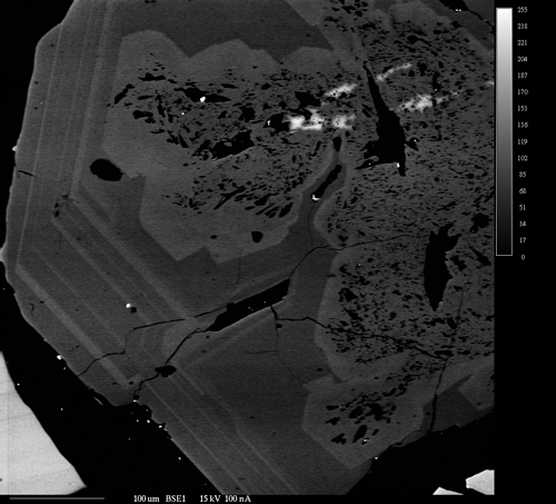
Backscattered Electron Imaging
Backscattered electron images show the differences in the average atomic number of materials within a sample. They are extremely useful in identifying the different phases that make up a sample and their relationships to each other. As the average atomic number of a phase depends on all the all the atoms present in that phase, BSE images reveal the overall chemical differences between the phases; as opposed to x-ray maps which show the differences in concentration of a single element in different phases. In addition, BSE images can usually be acquired much faster than x-ray maps. The two techniques are extremely complimentary in examining the makeup of heterogeneous samples.

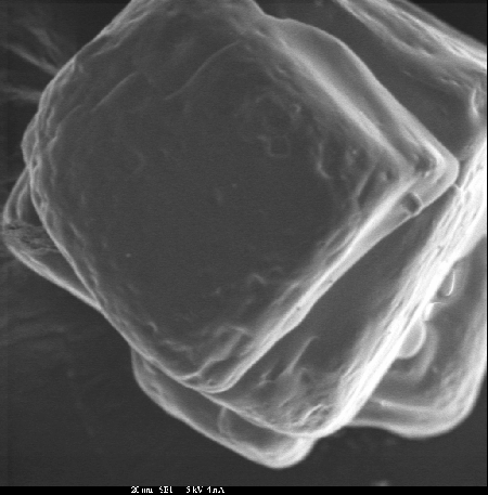
Secondary Electron Imaging
In secondary electron imaging, the electron microprobe is used as an electron microscope to provide a magnified image of the surface of a sample. The technique is useful in examining the features down to a few μm in size. Secondary electrons are formed when beam interaction with atoms in the sample causes loosely bound, low energy electrons (≤ 50 eV) to move through the sample. Due to their low energy, only secondary electrons formed near the point of beam impact can escape the sample and be detected which allows imaging of surface features. The pictures below are secondary electron images of grains of table salt taken at two different magnifications.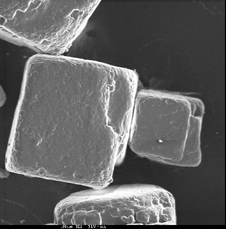
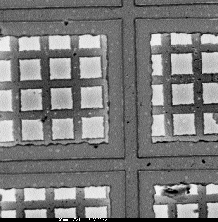
Absorbed Current Imaging
Absorbed current imaging provides a spatial image of the amount of beam current absorbed by the sample. Electrons in the beam that do not form backscattered or secondary electrons eventually lose their energy and are captured within the sample (unless the sample is very thin). These absorbed electrons produce an electric charge in the sample that must be conducted to ground. The current flowing to ground from the sample thus provides information similar to that of a combined backscatter electron and secondary electron image. The pictures below are absorbed current images of a grid made up of Cu (thick bars), Ag (thin bars), and chrome steel (substrate).